← Why Every Electronics Hobbyist Needs The Mecha Wiring: Eagle Free Download To Master Complex Wiring And Digital Hardware Designs - 10 essentials for every electronics hobbyist and tinkerer Your Essential Guide To The Vauxhall Corsa D Fuse Box Location And Accessing Complete Wiring Schemas Online - fuse box diagram opel/vauxhall corsa d (2006-2014) →
If you are looking for PCB Layout Design - ESP32 - — ESP Hardware Design Guidelines latest you've visit to the right web. We have 35 Images about PCB Layout Design - ESP32 - — ESP Hardware Design Guidelines latest like Some LVDS PCB Layout Guidelines For Ensuring Signal, 40% OFF, DDR5 PCB Layout, Routing, and Signal Integrity Guidelines and also LVDS-PCB-Layout-Guidelines für gute Signalintegrität | Altium. Read more:
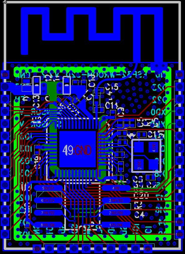
PCB Layout Design - ESP32 - — ESP Hardware Design Guidelines Latest
 docs.espressif.com
PCB Layout Design - ESP32 - — ESP Hardware Design Guidelines latest ...
DDR5 PCB Layout, Routing, And Signal Integrity Guidelines
 www.linkedin.com
DDR5 PCB Layout, Routing, and Signal Integrity Guidelines
Circuit Board Layout Services
 www.circuitdiagram.co
Circuit Board Layout Services
Redistribution Layer (RDL) Technology For ICs Package | Reversepcb
 reversepcb.com
Redistribution Layer (RDL) Technology for ICs Package | Reversepcb
Pcb Layout Vs Schematic Design » Wiring Diagram
 www.organised-sound.com
Pcb Layout Vs Schematic Design » Wiring Diagram
Top 5 PCB Design Rules You Need To Know | PCB Design Blog | Altium
 resources.altium.com
Top 5 PCB Design Rules You Need to Know | PCB Design Blog | Altium
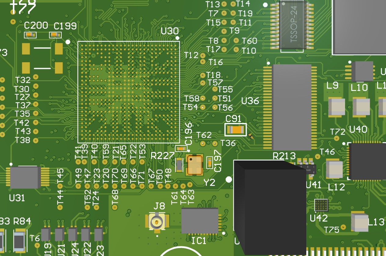
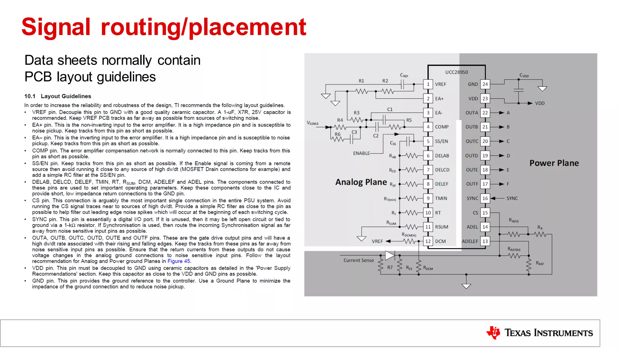
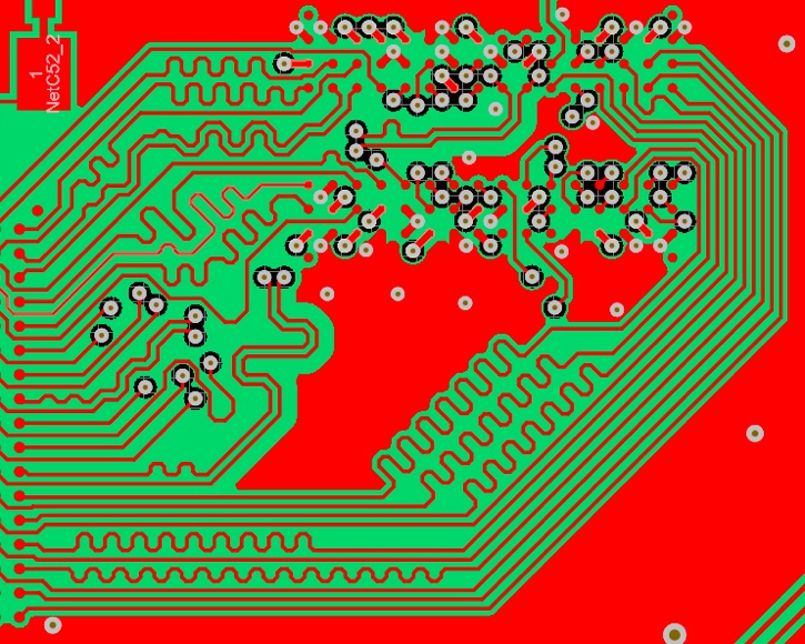
PCB Layout Guidelines.pdf
 www.slideshare.net
PCB Layout guidelines.pdf
Some LVDS PCB Layout Guidelines For Ensuring Signal, 40% OFF
 www.oceanproperty.co.th
Some LVDS PCB Layout Guidelines For Ensuring Signal, 40% OFF
How To Read PCB Layout Design: Beginner’s Guide
 www.viasion.com
How to Read PCB Layout Design: Beginner’s Guide
PCB Layout Guidelines | Design Rules & Requirements | Tips
 www.wellpcb.com
PCB Layout Guidelines | Design Rules & Requirements | Tips
LVDS-PCB-Layout-Guidelines Für Gute Signalintegrität | Altium
LVDS-PCB-Layout-Guidelines für gute Signalintegrität | Altium
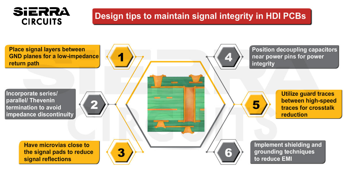
10 HDI PCB Design Tips For Signal Integrity | Sierra Circuits
 www.protoexpress.com
10 HDI PCB Design Tips for Signal Integrity | Sierra Circuits
PCB Layout Design - ESP32-C3 - — ESP Hardware Design Guidelines Latest
 docs.espressif.com
PCB Layout Design - ESP32-C3 - — ESP Hardware Design Guidelines latest ...
PCB Layout Design - ESP32-S3 - — ESP Hardware Design Guidelines Latest
 docs.espressif.com
PCB Layout Design - ESP32-S3 - — ESP Hardware Design Guidelines latest ...
[Schematic And PCB Review Request] SD Card Reader + PowerBank : R
![[Schematic and PCB Review Request] SD Card reader + PowerBank : r](https://preview.redd.it/schematic-and-pcb-review-request-sd-card-reader-powerbank-v0-domvov12o6y91.png?width=2350&format=png&auto=webp&s=52d3a53cd0ceae2a9f73daf26fa7785dfa08de4a) www.reddit.com
www.reddit.com
[Schematic and PCB Review Request] SD Card reader + PowerBank : r ...
How To Avoid And Suppress Signal Reflection In PCB - TechSparks
 www.tech-sparks.com
How to Avoid and Suppress Signal Reflection in PCB - TechSparks
PCB Layout Design - ESP32-C6 - — ESP Hardware Design Guidelines Latest
 docs.espressif.com
PCB Layout Design - ESP32-C6 - — ESP Hardware Design Guidelines latest ...
Impedance Control Of Vias And Its Influence On Signal Integrity In PCB
 www.raypcb.com
Impedance Control of Vias and Its Influence on Signal Integrity in PCB ...
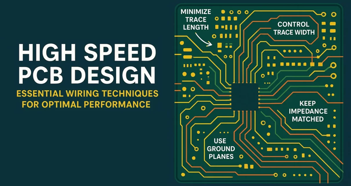
PCB Layout Guidelines For High Speed Applications
 www.linkedin.com
PCB Layout Guidelines For High Speed Applications
PCB Layout: A Comprehensive Guide - GlobalWellPCBA
 www.globalwellpcba.com
PCB Layout: A Comprehensive Guide - GlobalWellPCBA
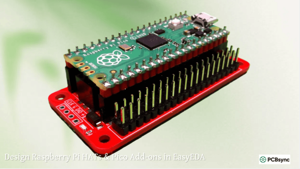
PCB Connector Design: Edge, USB-C & Micro SD Card Layout Guide - PCBSync
 pcbsync.com
PCB Connector Design: Edge, USB-C & Micro SD Card Layout Guide - PCBSync
Graphics Card PCB Layout: Everything You Need To Know – Hillman Curtis
 hillmancurtis.com
Graphics Card PCB Layout: Everything You Need to Know – Hillman Curtis ...
Pcb Design Guide | Applying IPC Standards To PCB Layout Design – EDNEU
 edge.adlershof-projekt.de
Pcb Design Guide | Applying IPC Standards to PCB Layout Design – EDNEU
DIY PCB Crafting: Minimalist Methods Guide
 www.zonetronik.com
DIY PCB crafting: Minimalist methods guide
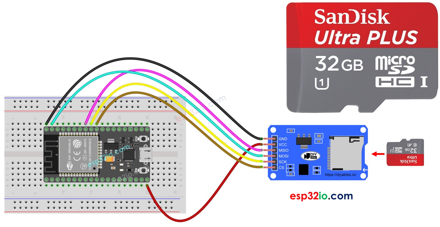
ESP32 - SD Card | ESP32 Tutorial
 esp32io.com
ESP32 - SD Card | ESP32 Tutorial
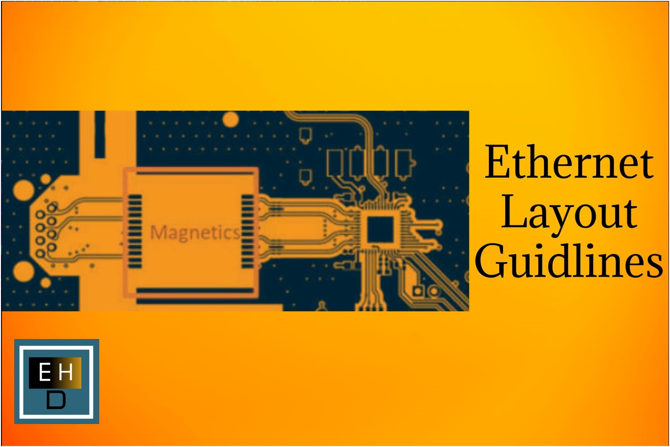
Ethernet PCB Layout Design Guidelines - Embedded Hardware Design
 embeddedhardwaredesign.com
Ethernet PCB Layout Design Guidelines - Embedded Hardware Design
Impedance Control Of Vias And Its Influence On Signal Integrity In PCB
 www.raypcb.com
Impedance Control of Vias and Its Influence on Signal Integrity in PCB ...
Pcb Design And Layout » Hackatronic
 hackatronic.com
pcb design and layout » Hackatronic
GPU PCB: Structure, Function & Design Insights - GlobalWellPCBA
 www.globalwellpcba.com
GPU PCB: Structure, Function & Design Insights - GlobalWellPCBA
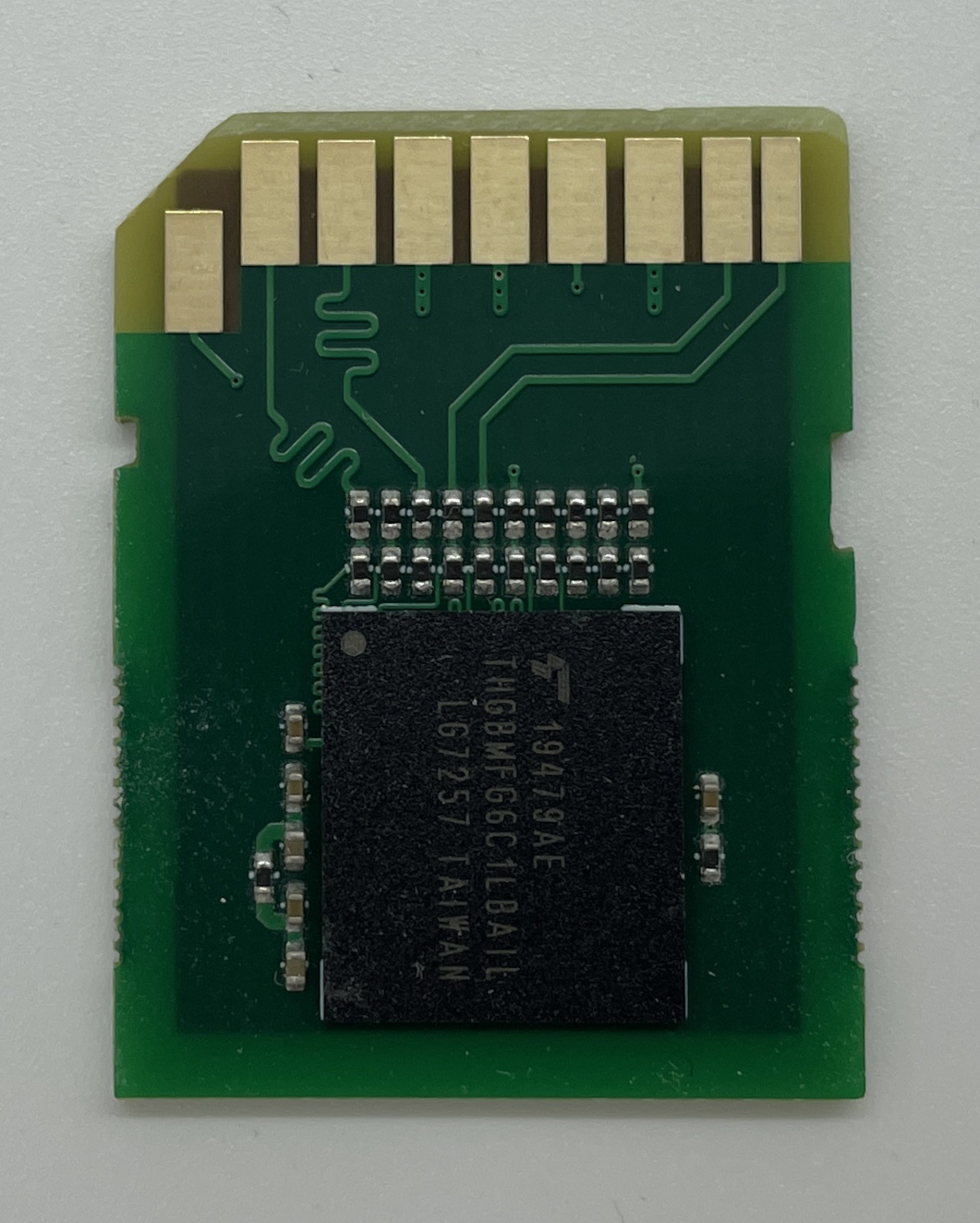
EMMC (micro)SD Card | KittenLabs
 kittenlabs.de
eMMC (micro)SD card | KittenLabs
Micro SD Card PCB Layout: Everything You Need To Know – Hillman Curtis
 hillmancurtis.com
Micro SD Card PCB Layout: Everything You Need to Know – Hillman Curtis ...
Basic Guidelines For Mixed-Signal Pcb Layout Design – MWCM
 www.blue-genes.de
Basic Guidelines For Mixed-Signal Pcb Layout Design – MWCM
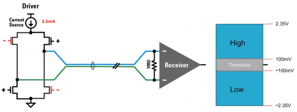
LVDS PCB Layout – Expert Guidelines You Need To Know! Pcb Layout Design
 superspotsz.blogspot.com
LVDS PCB Layout – Expert Guidelines You Need to Know! Pcb layout design ...
Essential Guidelines For Effective PCB Layout Design - ViasionPCB
 www.viasionpcb.com
Essential Guidelines for Effective PCB Layout Design - ViasionPCB
Getting Started With RF PCB Layout Guidelines
 www.hemeixinpcb.com
Getting Started With RF PCB Layout Guidelines
pcb design and layout » hackatronic. Impedance control of vias and its influence on signal integrity in pcb. Lvds pcb layout – expert guidelines you need to know! pcb layout design ...